


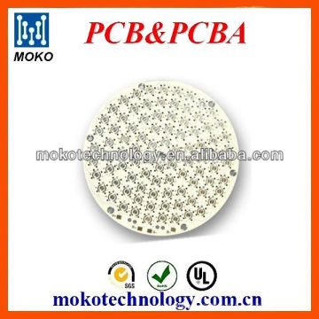

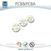
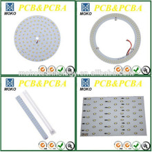
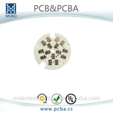
Aluminium basierte runde LED PWB-Versammlung
- Verpakung:
- Innere Verpackung: Vakuumverpackung Äußere Verpackung: Standardkarton
- Marke:
- MOKO
- Ort Von Zukunft:
- Guangdong China (Festland)
Basisinformation
Modell: MK40331BE06
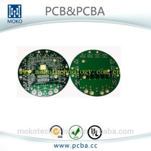
Produktbeschreibung
Spezifikationen 1. Angebot Probe \ n2.UL, SGS, Rohs CE \ n3.OEM & ODM PCB und PCBA \ n4.Hohe Qualität \ n5.Schnelle Lieferung \ n \ n Aluminium basierte Runde LED Platine \ n \ n MOKO Service einschließlich: \ n \ n 1.PCB \ n 2.Komponenten-Service \ n 3.PCB-Assembly / OEM-Service \ n 4.PCBA-Test \ n \ n \ n PCB Technische Spezifikation \ n \ n
\ n \ n \ n PCBA-Fähigkeiten \ n
\ n Technische Voraussetzung für Leiterplattenbestückung: \ n \ n1. Professionelle Aufputz- und Durchstecklöttechnik \ n2. Verschiedene Größen wie 1206,0805,0603 Komponenten SMT-Technologie \ n3.ICT (In Circuit Test), FCT (Funktionsprüfung) -Technologie. \ N4.PCB Montage mit UL, CE, FCC, Rohs-Genehmigung \ n5.Nitrogen Gas Reflow-Löten Technologie für SMT. \ n6.Hohe Standard-SMT- und Löt-Fertigungslinie \ n7. Mit hoher Kapazität verbundene Technologiekapazität der verbundenen Leiterplatte. \ N \ n Zitatanforderung für PWB- und PWB-Versammlung: \ n \ n1. PCB-Gerber-Datei \ n 2. BOM-Liste für PCBA \ n 3. Beispiel für PCB und PCBA \ n 4.Test-Methode für PCBA \ n \ n PCB-Vorlaufzeit: \ n \ n \ n
\ n produktbezogene \ n \ n \ n 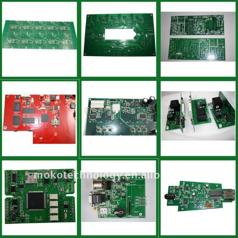 \ n
\ n  \ n \ n \ n \ n \ n Ansicht unserer Werkstatt \ n

 \ n
\ n  \ n \ n
| Number of Layer | 1,2,4 or 6,upto 18 layer |
| Order Quantity | 1 to 50,000 |
| Board Shape | Retangular,round,slots,cutouts,complex,irregular |
| Board Type | Rigid, Flexible, Rigid-flexible |
| Board Material | FR-4 glass epoxy, FR-4 high Tg, Rohs compliant,Aluminum,Rogers,etc. |
| Board Cutting | Shear,V-score,Tab-routed |
| Board Thickness | 0.2-4.0mm, Flex 0.01-0.25mm |
| Copper Weight | 1.0, 1.5, 2.0 oz |
| Solder Mask | Double-sided green LPI,Also support Red,White,Yellow,Blue,Black |
| Silk Screen | Double-sided or single-sided in white,yellow,black,or negative |
| Silk Screen Min Line Width | 0.006'' or 0.15mm |
| Max Board Dimensions | 20 inch*20inch or 500mm*500mm |
| Min Trace/Gap | 0.10mm, or 4mils |
| Min Drill Hole Diameter | 0.01'',0.25mm, or 10mils |
| Surface Finish | HASL,Nickle,Immersion Gold,Immersion Tin,Immersion Silver,OSP,etc. |
| Board Thickness Tolerance | ±10% |
| Copper Weight Tolerance | ± 0.25 oz |
| Minimal Slot Width | 0.12'', 3.0mm, or 120mils |
| V-Score Depth | 20-25% of board thickness |
| Design File Formate | Gerber RS-274,274D,Eagle and AutoCAD's DXF,DWG |
| Quantity | Prototype&Low Volume PCB Assembly,from 1 Board to 250,is specialty,or up to 1000 |
| Type of Assembly | SMT,Thru-hole |
| Solder Type | Water Soluble Solder Paste,Leaded and Lead-Free |
| Components |
Passive Down to 0201 size BGA and VFBGA Leadless Chip Carriers/CSP Double-sided SMT Assembly Fine Pitch to 0.8mils BGA Repair and Reball Part Removal and Replacement |
| Bare Board Size |
Smallest:0.25*0.25 inches Largest:20*20 inches |
| File Formate |
Bill of Materials Gerber files Pick-N-Place file |
| Types of Service | Turn-key,partial turn-key or consignment |
| Component packaging | Cut Tape,Tube,Reels,Loose Parts |
| Turn Time | Same day service to 15 days service |
| Testing | Flying Probe Test,X-ray Inspection AOI Test |
| PCB assembly process | Drilling-----Exposure-----Plating-----Etaching & Stripping-----Punching-----Electrical Testing-----SMT-----Wave Soldering-----Assembling-----ICT-----Function Testing-----Temperature & Humidity Testing |
| Single/double side | 4 layer | 6 layer | Above 8 layer | HDI | |
| Sample lead time(Normal) | 5-6 | 6-7 | 7-8 | 10-12 | 15-20 |
| Sample lead time(Fastest) | 48-72 hours | 5 | 6 | 6-7 | 12 |
| Mass production lead time(First batch) | 7-9 | 10-12 | 13-15 | 16 | 20 |
 \ n
\ n  \ n \ n \ n \ n \ n Ansicht unserer Werkstatt \ n

 \ n
\ n  \ n \ n
 Produktgruppe : LED-Beleuchtung PCBA
Premium Related Products
andere Produkte
heiße Produkte
Professional Aluminium pcb Lieferant für LEDKundengebundene Energiebank PCB, PWB-Versammlungsservice in ShenzhenPower Bank PCB Board und Leiterplattenmontage Hersteller in GuangdongODM Sim808 modul pcb gps tracker design serviceSchlüsselfertige Fabrik für flexible Schaltkreise in ChinaOEM-PCB elektronische Gestaltung Komponente supplerKundenspezifischer FR4 GPS Verfolger PCBA mit AntenneEinstellbare Elektroheizung Thermostat PCB PCBA Platine OEM HerstellerLeiterplattendesign für BLE-Modul, BLE-Gerät, BLE-ProjektEine stopp BLE smart drahtlose smart sex spielzeug ODM & OEM, smartphone APP kontrollierten frauen sex spielzeug Bluetooth modul PCB bord designIntelligentes Bluetooth drahtloses BLE-Modul PWB-Brettentwurf, bewegliche APP kontrollierte intelligente Ei-Vibrator PWB-Herstellung u. VersammlungBluetooth Anti verlorener Alarm Bluetooth Schlüsselsucher mit kundengebundenem ServiceProfessioneller Bluetooth Empfänger Bluetooth Tracker für Smart Key FinderKundengebundener Qualitäts-automatischer Hauptlösungsanbieter / HerstellerShenzhen Fast Printed Leiterplattenbestückung HerstellerSchnelles Shenzhen FR4 UL druckte PWB-Leiterplatte-Versammlung SMT u. DIP-Fabrik